A shield that worked well in one generation of telecom hardware can become less reliable in the next. The material may still be conductive. The enclosure may still look sealed. The EMI gasket may still appear compressed. The problem is that high-frequency hardware leaves less room for small physical gaps, weak contact points, and uncontrolled RF energy inside the device.
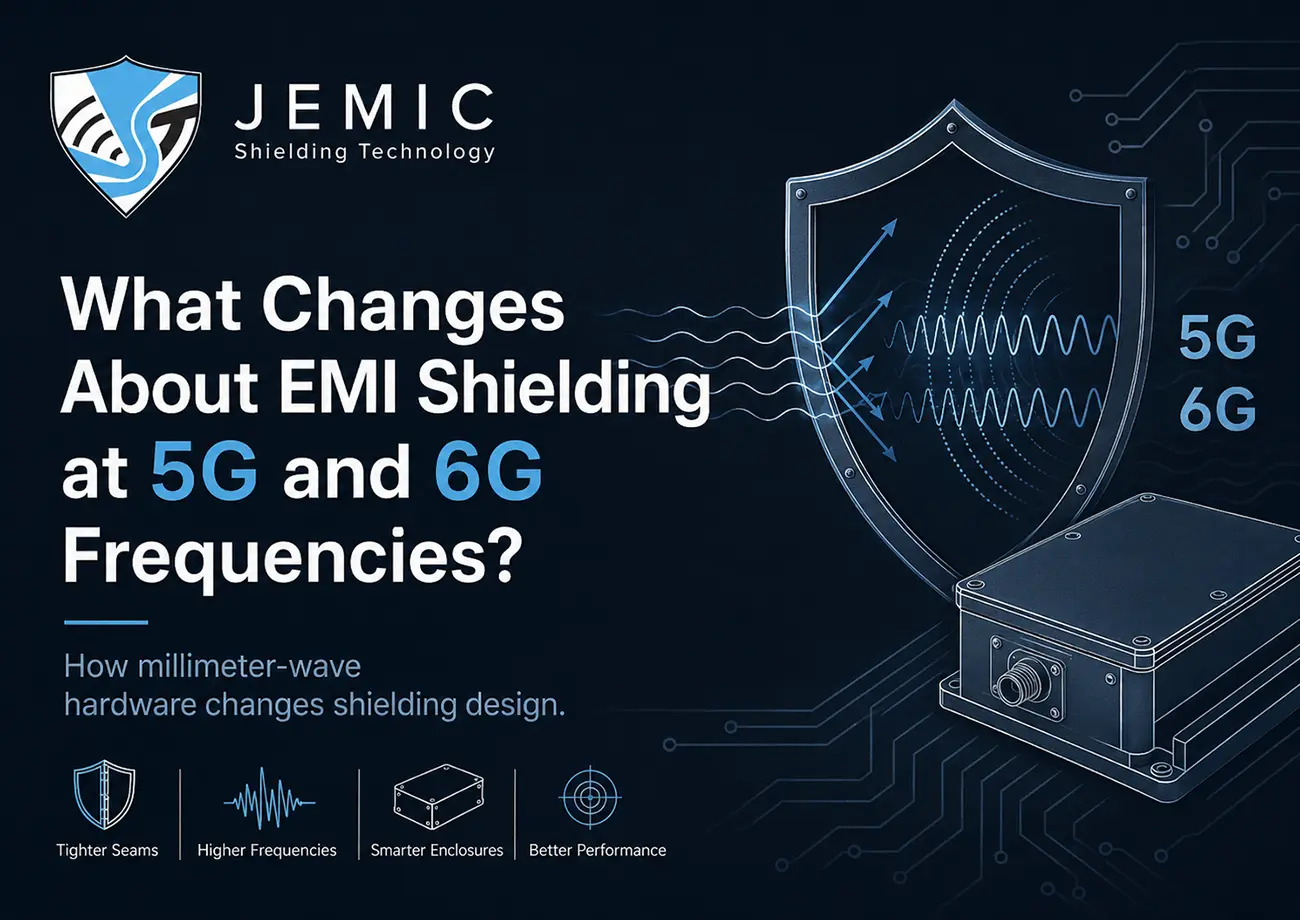
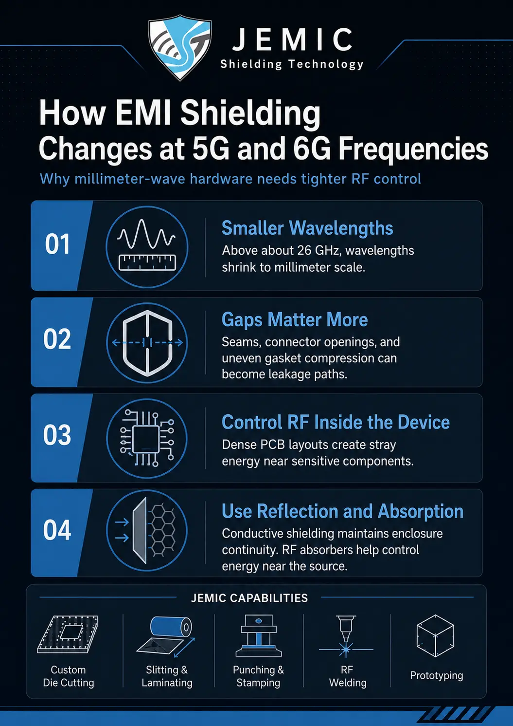
That is the practical issue behind 5G and future 6G shielding. As telecom hardware moves into millimeter-wave frequency ranges, wavelengths shrink, and the scale of the problem changes. A seam, connector opening, access panel, or uneven EMI gasket compression point that looked minor at lower frequencies can matter more at higher frequencies. The answer is not to move away from EMI shielding. The answer is to make EMI shielding more application-specific, using the right conductive materials, the right RF-absorbing materials, and the right finished part construction.
The Modern Problem Is Tighter RF Control
Older telecom equipment gave engineers more physical tolerance in many shielding designs. Small enclosure gaps, access panel seams, connector openings, and uneven EMI gasket compression points did not always create the same level of risk at lower frequencies. Many earlier telecom systems operated in frequency ranges where the wavelength was much larger than the small mechanical details inside the enclosure. That made the shielding problem more forgiving.
High-band 5G changes that assumption. The International Telecommunication Union identified additional bands for 5G, including 24.25 to 27.5 GHz, 37 to 43.5 GHz, 47.2 to 48.2 GHz, and 66 to 71 GHz. Those frequency ranges move the discussion into millimeter-wave behavior, where physical details become more important. The shield has to work more precisely with the enclosure, gasket profile, compression target, and board layout.
The issue also moves inside the device. Dense PCB layouts and high-frequency signal sources create stray RF energy near sensitive components. If that energy reflects around the inside of the enclosure, it can affect nearby chips, traces, shields, and signal paths. The enclosure still needs reflective shielding, but the internal RF behavior also needs control.
The design issues are not abstract. They show up in the same places engineers already evaluate during enclosure, board, and EMI gasket design.
| Design Concern | What Changes at Higher Frequencies | Why It Matters |
| Enclosure Seams | Small gaps become more important | Leakage risk increases as wavelengths shrink |
| Gasket Compression | Uneven contact becomes harder to ignore | The shield depends on consistent electrical continuity |
| Connector Openings | Small openings can become RF paths | The physical opening can affect shielding performance |
| PCB Layout | Stray RF energy stays close to sensitive parts | Internal interference can occur near the source |
| Material Conversion | Shape, thickness, and adhesive stack matter more | The finished part must match the real device |
The Direct Answer: EMI Shielding Becomes More Application-Specific
At 5G and 6G frequencies, EMI shielding changes because the shield becomes part of the RF design. The part is no longer only a conductive filler between two surfaces. It has to match the frequency range, enclosure geometry, board layout, compression profile, adhesive construction, and exposure conditions. That is the direct answer.
Reflective shielding still performs a major role. Conductive gaskets, tapes, foams, coatings, and elastomers help protect enclosures, panels, seams, doors, vents, wire entry points, connectors, and access covers. These materials support the Faraday cage effect by redirecting unwanted electromagnetic energy. That approach remains central to EMI shielding in telecom hardware.
The newer pressure comes from internal stray energy. At millimeter-wave frequencies, unwanted RF energy can reflect within compact electronics rather than leaving the device cleanly. That makes the inside of the enclosure less like an empty shielded box and more like a space where signals can bounce between nearby surfaces. Engineers still need reflective shielding, but they also need a way to control RF energy near the source.
RF-absorbing materials address that part of the shielding problem. Carbon-based or ferrous absorbers help reduce unwanted RF energy near chips and signal-generating components. They do not replace conductive shielding. They use conductive shielding to control energy that reflection alone may not address within dense hardware.
Before selecting or converting a shielding part, engineers should define the actual conditions the part must meet.
- Operating frequency range, including any high-band or millimeter-wave exposure
- Enclosure seams, connector openings, access panels, vents, and wire entry points
- Gasket cross-section, compression target, and contact surface condition
- Board-level areas where stray RF energy needs control near the source
- Environmental exposure, including heat, humidity, vibration, salt fog, and compression set
- Validation needs tied to the real part shape, not only the base material
Those details matter because the shielding strategy is no longer just a material decision. A conductive elastomer, foam, tape, coating, or absorber still needs to work in the actual device. The part needs the right shape, thickness, adhesive construction, clearance, compression, and placement. At high frequencies, those details affect performance.
Why the Finished Part Matters
A material data sheet does not answer the whole shielding question. It may show strong performance under controlled conditions, but the final device introduces additional variables such as geometry, compression, aging, assembly, and exposure. A gasket can fail to maintain contact. An adhesive can lose strength in humidity. An absorber can be placed too far from the signal source. A converted part can be cut correctly as a drawing but still miss the practical needs of the hardware.
Testing also must match the problem. IEEE Std 299 gives a recognized method for measuring shielding effectiveness, with published scope from 9 kHz to 18 GHz and extension paths up to 100 GHz for certain enclosure conditions. For millimeter-wave telecom hardware, the useful question is not whether testing matters. The useful question is whether the test range, part geometry, gasket cross-section, and environmental exposure match the real application.
NIST millimeter-wave research has focused on measurement and modeling at ranges such as 28 GHz, 60 GHz, and 83 GHz. That reinforces the same point from another direction. High-frequency performance depends on measurement context. Engineers need data that reflects the operating range and device environment.
The manufacturing side matters for the same reason. A shielding material must be a repeatable part that fits the enclosure, access panel, connector area, board cavity, or signal source location. For 5G and 6G hardware, that conversion step is part of the shielding solution.
What Engineers Should Take Away
5G and 6G do not make EMI shielding less important. They make it more precise. Smaller wavelengths make small gaps matter more, and dense electronics make internal stray RF energy harder to ignore. The shield still matters, but the design around it needs to be more specific.
The practical answer is application-specific shielding. Engineers need conductive materials to maintain enclosure continuity, RF absorbing materials to control energy near the source, and precision manufacturing to turn those materials into finished parts. That means the right material, geometry, compression, adhesive stack, placement, and validation method all have to work together.
JEMIC helps bridge that gap between material selection and a finished shielding component. The company supports telecom shielding applications through design support, prototyping, testing support, and in-house manufacturing services. At millimeter-wave frequencies, those details are not extras. They are part of what makes the shielding solution work in the final device.